
The Physics of Semiconductors That’ll Guide Your Understanding of Solar Cells

Introduction
The versatility in the availability of semiconductor materials for PV applications is the ability to alter their conductive properties. To do so, one must have an understanding of the basics of semiconductor technology and what they’re comprised of. In addition, conductivity can also be varied through the alteration in the bandgap, impurities and even the application of high temperature. You might be overwhelmed with all this information but we have got you covered!
Through this article, we aim to guide you into an understanding of what semiconductors are made of which will be explained by diving into the microscopic world of atoms that make up a crystal structure. We will then follow up with how ‘carriers’ are generated for conduction and the significance of a concept called ‘bandgap’. We will also cover the parameters taken into consideration that can affect conduction which is called as n-type and p-type semiconductors achieved through doping. So with this article, you’ll soon be able to justify the basics of semiconductor physics and how they’re important when considering solar technology!
Silicon as a Semiconductor
Semiconductor materials are comprised of either group IV, or a combination of groups III and 5, or a combination of groups II and VI. These groups vary in terms of properties and usually researchers take advantage of these variances to optimize an efficient material for PV applications. Although semiconductor materials are made of different groups in the periodic table, they share certain characteristics which make them similar to be classified as semiconductors and the most common material used in the PV industry is Silicon which is a group IV material. To make the understanding of the structure easier, let’s take the example of silicon.
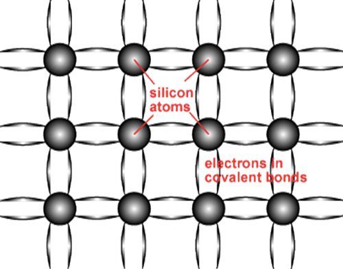
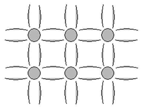
Silicon contains atoms which are bound together in a uniform structure. Hence, it’s known as a crystalline structure because the atoms are arranged in an orderly fashion. Each atom of silicon contains 4 valence electrons which are covalently bonded or shared with 4 other silicon atoms. So each silicon atom is surrounded by 8 electrons which are a part of the covalent bonds present in the crystal lattice .

Bandgaps of Semiconductors
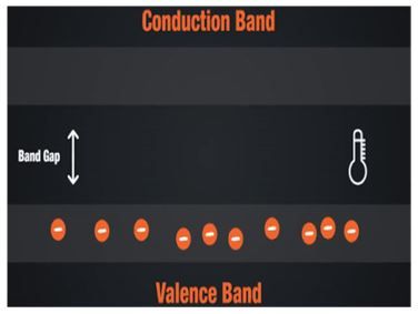
The bandgap of a material is defined as the minimum amount of energy needed by an electron to break free from its bound state.
To understand bandgaps better, consider a cluster of identical atoms which are separated from each other such that there are no interactions between them. These cluster of atoms form bands called as the valence band and the conduction band separated by a distance called as ‘bandgap’ or the ‘forbidden gap’ which is the energy gap between the bound state/valence band and the free state/conduction band.
Valence band can be defined as a state where electrons are contained at lower energy levels. Conduction bands are called as such because it’s always partially occupied with electrons making them conducive for conduction of electricity. When the required amount of energy is met, the electrons break free from its bound state and gets excited from the valence band to the conduction band and becomes ‘free’ to participate in conduction.
Correspondingly, the space that is now created from the electron escaping into the conduction band is now occupied by a hole where the electron was formerly bound. This hole can also be used for conduction. Electrons and holes together are termed as charge carriers. This is an important parameter as it determines how much current can be generated from that particular semiconductor that’s been fabricated to make a solar cell.
The bandgap nature at 0Ko determines what kind of material is being used; whether it’s a conductor, an insulator or a semiconductor. If the material is a conductor, then the conduction band will be full of electrons and the valence band will be empty. Metals are good examples of conductors. If it’s an insulator, the valence band will be full and the conduction band will be empty because insulators don’t conduct current.
Materials such as glass and wood are good examples of insulators Semiconductors are also similar to insulators where the conduction band is empty but the valence band is full, however, the difference in the gap between the valence band and conduction band is smaller than insulators which makes it easy for electrons to jump into the conduction band.
This transfer of electrons from band to band can be achieved through the application of temperature which provides sufficient thermal energy to transfer the electrons from valence band to conduction band. Apart from thermal energy, electrons can be transferred to the valence band through the absorption of light energy. Absorption of light energy deals with photons which are particles that comprise light energy. Absorption of light is discussed in a separate article
Conduction in Semiconductors
Now since we’ve understood what makes a semiconductor material, it is important to talk about the conduction that takes place within a semiconductor for the operation of a solar cell.
At low temperatures, semiconductors such as silicon, act as an insulator whereas, at higher temperatures, it acts as a conductor. This is because, at higher temperatures, the electrons in the material have sufficient energy to break away from their covalent bond and get excited to a higher energy level which in this case is the conduction band. Once the electrons are in the conduction band, they can freely move around in the lattice concurring with the conductive property of the semiconductor material. Generally, semiconductors can conduct current at room temperature. Only at 0Ko, does the semiconductor behave as an insulator. The conductive nature of the material aids engineers and researchers to decide on the best semiconductor that can be used for PV applications.
Electrons are considered to be in low energy state when it is bound to other atoms. At this stage, it cannot participate in conduction. When electrons are free to move in the lattice after excitation, it’s considered to be in high energy state with a hole left behind in the valence band. Electrons possess negative charge and holes possess positive charge
Therefore, when it comes to the conduction mechanisms of semiconductors, we must take into consideration the bandgap, the number of electrons or holes (charge carriers) available for conduction and the generation of electron-hole pairs with the possibility of recombination. The concepts of generation and recombination are explained in another article.
Intrinsic Carrier Concentration
We have covered the basics of semiconductor materials, its structure and the conduction that takes place within a semiconductor material. Now we need to understand more on the electrons or holes that are used for conduction and how they are significant in the operation of solar cells.
Electrons and holes that partake in conduction are called intrinsic carriers. The number of electrons and holes available for conduction are contingent upon 2 conditions:
- Temperature
- Bandgap
As the material is thermally excited, free carriers are generated in both the bands. The concentration of these carriers is characterized as intrinsic carrier concentration and it is denoted with the letter ‘n’. The term intrinsic is used because these materials do not have any impurities added to it to increase its conductivity. Addition of impurities is called doping and it will be discussed at the end of this article. Since no impurities are added, the material is free from external factors that contribute to conductivity and are operated only by carriers that are generated by the material intrinsically leading to the name-Intrinsic materials.
The intrinsic carrier concentration is also dependent on the bandgap of the material. If the bandgap of the material is large, then the carriers may not have enough energy to break the bond and get excited to a higher energy state. Therefore, the intrinsic carrier concentrations are quite low in materials with high bandgaps. On the contrary, when the semiconductors are subjected to high temperatures, the intrinsic carrier concentration increases because more energy is provided for electrons to break the bond and get thermally excited to a higher energy level.
Silicon’s intrinsic carrier concentration has been extensively studied for research and development purposes and it was concluded that at 300K, the intrinsic carrier concentration for Si, denoted by ni, is 9.65 x 109 cm-3. This value was obtained through modelling studies and it has been accepted as a general value that’s commonly used for calculation purposes. This value is also subject to experimental error. Intrinsic carrier concentration has a measured increase for solar cells calculated at 25oC. These cells have a value of 8.3 x 109 cm-3.
The formula derived for the calculation of intrinsic carrier concentration is given by:
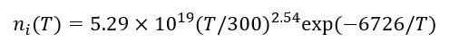
Where ni = Intrinsic carrier concentration of the semiconductor material
T=Temperature in Kelvin
Therefore, the intrinsic carrier concentration plays a significant role in the conduction of semiconductor material. However, the intrinsic nature of semiconductors is limited only to certain types of semiconductor materials. Depending solely on intrinsic carrier concentration will limit the achievement of high efficiency. Therefore, the technique of doping will help in limiting drawbacks associated with the exclusivity of materials with high intrinsic carrier concentrations
Doping in Semiconductors
Doping is a method that helps in varying the number of electrons and holes present in a semiconductor. It is a technique wherein we add or dope impurities from other materials to increase the conductivity of the material. The process of doping not only helps with conductivity but also helps to balance the number of electrons and holes present in a crystal lattice by shifting the balance between the two. There are 2 types of materials that are created with the help of doping:
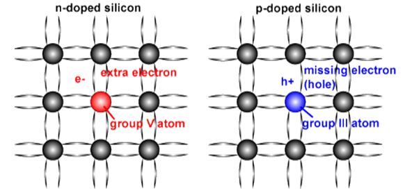
- Creation of N-type materials when group IV materials are doped with group V materials.
- Creation of P-type materials when group IV materials are doped with group III materials.
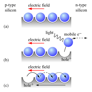
N-type materials are those materials which have an excess of electrons available for conduction. N-type materials are comprised of elements from group V of the periodic table. Group V elements have 5 valence electrons and form covalent bonds with 4 valence electrons of silicon. Hence, there is an extra valence electron present in the lattice which is available for participation in conduction. These extra electrons add more to the free carriers present in the conduction band and help to increase the overall conductivity of the material.
P-type materials have an excess number of holes available for conduction. P-type materials belong to group III elements of the periodic table and have only 3 valence electrons available for forming covalent bonds with silicon atoms (Si atoms have 4 valence electrons). This leads to a lacking in the number of electrons because there aren’t enough electrons available for covalent bonding. Hence, the formation of a hole takes place which increases the number of holes available for conduction. Since there is a disparity in the valence electrons available for covalent bonding, we can see that all the available electrons are bound through covalent bonding thereby increasing the number of holes present.
In the case of doped materials, one type of carrier always exceeds than the other. Either electrons are in excess or holes are in excess. Therefore, the carrier that is in excess is called as majority carriers and the carriers that are low in concentration are called as minority carriers.
The table summarizes the gist of doping and the types of semiconductors available when doped or added with impurities to increase the conductive property of the material
| P-type (positive charge) | N-type (negative charge) | |
| Dopants | Group III such as Boron | Group V such as Phosphorous |
| Bonds | Excess holes | Excess electrons |
| Majority Carriers | Holes | Electrons |
| Minority Carriers | Electrons | Holes |
Conclusion
As we conclude this article, we have been able to get a broad understanding of the basics of semiconductors and semiconductor physics that play a significant role in the operation of a solar cell. We were able to develop an understanding from the creation of semiconductor materials which included the materials and structure, to a base on conduction and conduction requirements of a semiconductor material which aid the collection of current and thus learning its significance in the efficiency of solar technologies. In this day and age, it is essential to understand alternative options that can meet our energy demands and one such option is solar technology. As we progress forward, we can see depletion the non-renewable resources that we heavily depend upon. So we must consider options that are sustainable for a bright future because, in the end, it is not only humankind that is being benefitted from this positive change, but the environment as well.