The Ultimate Guide to Semiconductor Junctions

Introduction
When we consider the physics of solar cells, we must consider the existence of junctions. These junctions exist between the different materials of different doping concentrations of a solar cell. Solar cells are composed of both p-type and n-type semiconductors which are combined together to form a p-n junction.
This junction allows the process of photovoltaic effect to take place. Light of suitable wavelength interacts with the semiconductor material of the solar cell by transferring a photon. Photon’s energy gets transferred to the semiconductor atoms which create electrons and holes which move to opposite sides of the semiconductor due to the presence of an electric field.
The movement of electrons to the p-side and holes to the n-side helps in aiding generation of current in the cell. Different types of semiconductor junctions aid the operation of a solar cell.
The most common semiconductor junction is known as the p-n junction which will be detailed as we go further into this article. A p-n junction that is fabricated from the same semiconductor material, such as crystalline silicon (c-Si), is known as PN homo-junctions. A p-n junction fabricated from different semiconductor materials with different chemical compositions is known as PN hetero-junctions. There’s a p-i-n junction wherein an intrinsic layer is inserted between the p-type layer and the n-type layer to generate an electric field that will extend the region for available conduction.
There’s also a metal-semiconductor junction in which an interface is formed when a metal and a semiconductor material are joined together leading to the formation of a Schottky barrier. The availability in the variations of solar cell junctions operates under the guise of the concept of a p-n junction which forms the base of all other types of junctions. P-N junctions can separate the electrons and holes to generate voltage within a solar cell and produce useful work.
This article will focus on the basics of p-n junctions such as the formation of p-n junctions, junction diodes, p-n junction biasing and diode equations which are considered to be important for the effective functioning of a solar cell.
Basics of P-N Junctions
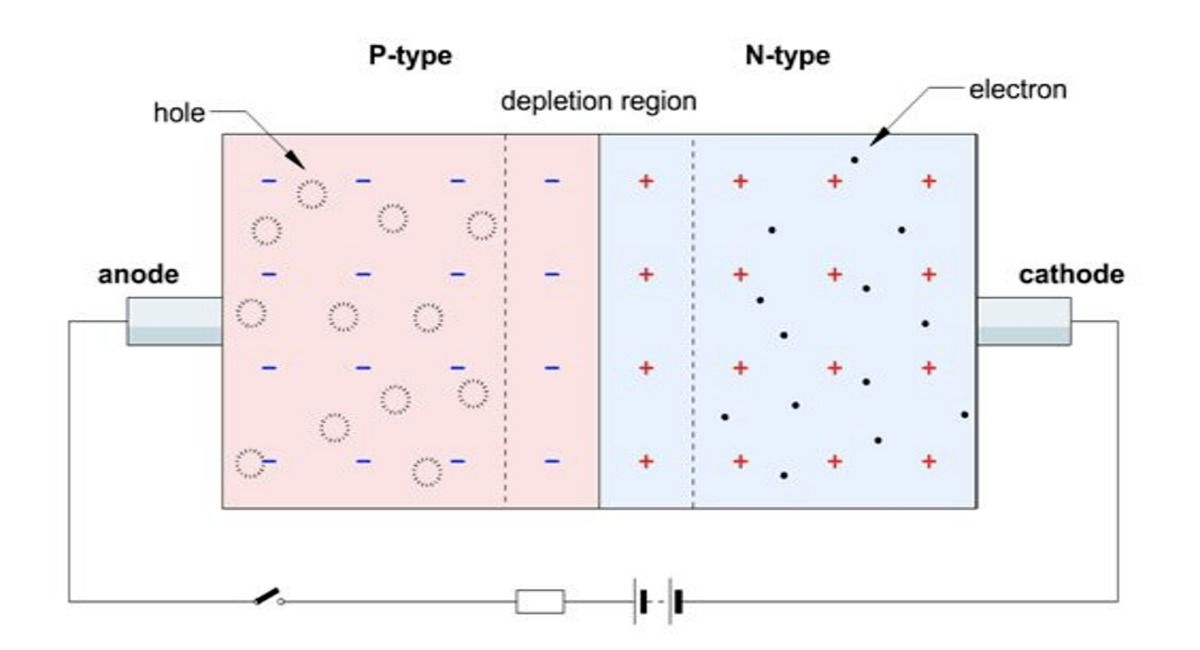
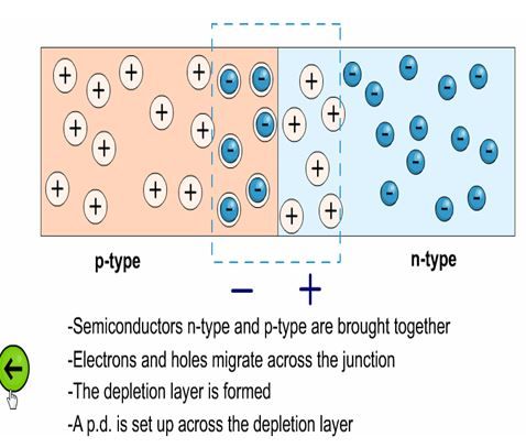
The formation of a p-n junction requires the joining of the n-type material and the p-type material of the semiconductor. The excess number of electrons and holes from n-type and p-type respectively causes an overall net movement of carriers called diffusion which is detailed in another article.
Basically, the excess electrons from n-type material diffuse into the p-type material which exposes positive ion cores and the diffusion of holes from p-type material to n-type material expose negative ion cores. This process leads to the formation of an electric field at the interface of the p-type and n-type materials and forms a depletion region.
The presence of an electric field induces the formation of voltage at the junction. The depletion region is called as such because it doesn’t retain carriers and instead, swiftly sweeps them out to either side of the junction. So the depletion region is depleted or empty from the presence of carriers such as electrons or holes.

To understand p-n junctions further, we must first understand the concept of a diode. A diode is, simply put, a device usually made from semiconductor materials that have 2 terminals. These terminals conduct current only in one direction whereby there’s low resistance in one direction enabling passage of current and high resistance in the other direction.
The foundation of p-n junction diodes is not only the base of solar cells but of many other electronic devices such as bipolar junction transistors, LEDs, lasers, etc. Therefore, a p-n junction diode is a fundamental operation of almost all electronic devices combining all processes of carrier transport, generation and recombination which are explained in another article.
Usually, the electric field generated obstructs the transfer of carriers across the junction. Even if the electric field inhibits the crossing of majority carriers across the depletion region, they still can transfer through.
However, minority carriers are unable to do so because they undergo drift transport which sweeps them across the depletion region. The transfer of carriers takes place until equilibrium is achieved. Equilibrium is when the net current of both diffusion and drift (explained in another article) is 0 and the drift current is equal and opposite to the diffusion current generated across the semiconductor.
The electron diffusion current and the electron drift current balance and cancel each other out. Similarly, the hole diffusion current and the hole drift current balance and cancel each other out. These conditions lead to a state of equilibrium where there’s no net current.
A state of equilibrium is represented between the generation of carriers, recombination, diffusion and drift when there are no external inputs applied or added in the presence of an electric field at the depletion region. Even if the electric field obstructs the pathway of carrier diffusion, some carriers still manage to cross through the junction through the process of diffusion.
Statistically speaking, some carriers have a high velocity which enables them to cross the junction. Once a majority carrier crosses the junction, it becomes a minority carrier since the diffusion is taking place where negatively charged carriers cross over to p-type material which is positively charged and vice versa. These carriers diffuse away from the junction to the opposite sides and will travel a distance called as the ‘diffusion length’ before which they recombine.
Recombination is when an electron recombines with a hole and emits energy which leads to the loss in the number of available carriers for conduction. The current that is generated due to the diffusion of charge carriers across the junction is known as diffusion current. Correspondingly, minority carriers that are transported to the diffusion region’s edge are often swept or carried across the diffusion region by the electric field at the depletion region. The current generated from this process is known as ‘drift current’.
Minority carriers which are thermally generated at the junction within the diffusion length often limit the drift current in the state of equilibrium.

Bias of P-N Junctions
Since we have understood the basic functioning of a p-n junction diode, it is now essential to understand the biasing of p-n junctions. There are 3 types of operation in semiconductor devices. They are:
Thermal Equilibrium: At this state, no external inputs such as applied voltage or light are applied. The currents that exist within the device balance and cancel each other out such that there is 0 net current in the device.
Steady State: At this state, external inputs such as applied voltage or light are applied but the conditions remain unchanged with time. Usually, steady-state conditions are considered to operate in devices that are in either forward bias or reverse bias which shall be explained further in this article.
Transient: This is the last type of operation mode where there is a short delay in the response of a solar cell if the applied voltage changed rapidly. Solar cells are generally not accustomed for high-speed operations so there are cases where transient effects like delayed response time can occur within a solar cell which needs to be considered during calculation and operation of solar cells.
As mentioned before, semiconductor devices usually calculated at steady state operate under different biases. There are 2 types of p-n junction or semiconductor biases:
- Forward bias
- Reverse Bias
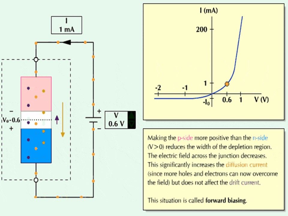
1] Forward bias: It takes place when the electric field generated across the solar cell is decreased as a function of an applied voltage. Forward bias helps in increasing the diffusion current by providing ease with which carriers diffuse across the depletion region. Recombination rates increase in the presence of an external circuit which provides majority charge carriers continuously.
This leads to a decrease in the influx of charge carriers and an increase in the diffusion rates. Ultimately, the current is increased across the depletion region in the solar cell. When the diode is in forward bias, the application of negative voltage to the n-type material and positive voltage to the p-type material leads to the formation of an electric field which is in an opposite direction to that of the depletion region.
Also, the limited number of carriers present in the depletion region is in alignment with the fact that the resistivity of the depletion region is high. This high resistivity leads to a drop in the electric field across the depletion region. This is significant because the net electric field is the difference in the applied field and the electric field across the depletion region. So these parameters lead to an overall reduction in the net electric field.
The reduction in the electric field also affects the equilibrium achieved at the junction which results in decreasing the barrier to carrier diffusion from one side to another and increasing the diffusion current. As diffusion current increases drift current remains virtually unchanged as it depends on the number of carriers generated at the depletion region within the length of the diffusion length.
The width of the depletion region is reduced only by a little; therefore the number of minority carriers that are swept or transported across the junction remains principally unchanged.
An increase in the minority carrier influx at the depletion region edge is observed when there is an increase in the amount of diffusion taking place from one side of the junction to another. The process of diffusion leads these carriers away from the junction and will in due course recombine with a majority carrier.
The external circuit provides the majority carriers and hence, there is a net flow of current in forward bias. Assuming the condition where there is no recombination; in such a case, the diffusion of carriers from one side to another will finish and the minority carriers will reach a new state of higher equilibrium concentration.
Higher the rate of recombination achieved, higher is the flow of current across the junction because as more minority carriers that are injected recombine with majority carriers, more carriers can diffuse across the junction.
As a result, we can consider the diffusion current obtained in forward bias to be the recombination current flow. There is one extremely important parameter called the ‘dark saturation current’. This current is represented as Io and plays a major role in distinguishing diodes from each other. Io helps to measure the recombination that takes place in a device so higher the recombination, larger is the Io value. This parameter needs to be measured during the application of forward bias since it’s associated with the recombination process that takes place within a solar cell.
2] Reverse bias: It takes place when the electric field is increased as a function of the applied voltage across the solar cell. In reverse bias, diffusion current decreases significantly. When a reverse bias is applied, the larger electric field makes it harder for carriers to diffuse from one side to another.
Hence, there is a decrease in the diffusion current. Just like in forward bias, the number of minority carriers present in both p-type and n-type sides of the p-n junction limits the value of drift current and remains unaffected with the increase in the electric field. A 2nd order effect in solar cells contributes to a small increase in the drift current due to a slight increase in the width of the depletion region, however, the change is negligible. If we are considering thin-film solar cells, a change in the width of the depletion range significantly affects the operation of solar cells because usually the depletion region is only around half the solar cell’s thickness but this is a topic for another day!

Diode Equations
Finally, we come to a section called diode equations which helps in the calculation of various parameters in a solar cell which is discussed below.
The first equation is given by the Ideal Diode Law. This equation gives the formula for current as a function of voltage that flows through a diode:

Where:
I = The overall current that flows through the p-n junction diode;
Io = Dark saturation current which is directly affiliated with recombination. It’s inversely proportional to the quality of the material and hence negatively affects the efficiency of solar cells. This is the current that ‘leaks’ in a diode in the absence of light.
q = Electron charge (this is an absolute value);
V= Voltage that is applied across the terminals of the p-n junction diode;
k = Boltzmann constant;
T= Absolute temperature (given in Kelvin);
It is important to note that at 300K, kT/q has a value of 25.85 mV which is considered as the ‘thermal voltage’.
Also, Io increases as temperature increases. Io decreases with an increase in the quality of the material.
For non-ideal diodes, the equation is given as:

All variables remain the same except with an addition of a term in the denominator of the exponent called ‘ideality factor’. Ideality factor is denoted with ‘n’ and is a value that’s usually between1 and 2. The value of the ideality factor increases as the current flowing through the diode decreases. An increase in the ideality factor would significantly increase the value of the dark saturation current as well, so if a device has a high ideality factor, the device would typically have a low turn-on voltage
Conclusion
We hope that this article provided you with a base on how diodes and semiconductor junctions operate a solar cell. From the moment a p-n junction is formed, to the carrier movement in equilibrium in the diodes, we can understand the factors that need to be considered in solar cell technology. We were also able to give a broad overview of the bias of p-n junction diodes and the implications of each type of biases.
We ended the bulk of our article with some equations of current flowing through a diode under ideal and non-ideal conditions. These equations extrapolated on the importance of the different terms in the equations given and how they contribute to the quality of a solar cell. Therefore, we hope that with this article, you’ve gained a baseline understanding of what forms the operation of our future technological contenders of the energy industry!

